Areas of Application
• Redistribution layers (RDL) for opto- and microelectronics
• Solder, Cu and Au bumps & UBM for backend device manufacturing
• Functional metallic layers for MEMS
• Interconnections as Cu pillars, TSVs for packaging
• Blind vias
• Micro forming and moulding for microsystems
Features and benefits
Process stability & control
• Control of uniformity
• Electrolyte booster for lifetime enhancement
• pH-control
• Automated dosage
• Logging of process parameters
Operator & service safety
• Good accessibility
• Easy maintenance
• Drag out rinse included in plating process module
Flexibility
• Different substrate sizes
• Adjustable wafer thickness
• Wide range of materials
• Flexible recipe management
High quality plating performance
• Inert or soluble anode
• DC or forward/reverse pulse plating
• Edge exclusion: < 3mm
• 360° Ti contact pin arrays
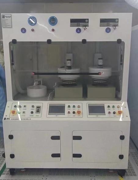
Technical Data
Dimensions 600 x 1600 x 2050 mm per module (length x width x height)
Wafer thickness 350 - 1000 μm
Wafer size 4“ - 12“ wafer
Wafer material Si, SiC, InP, SiGe, glass, sapphire, ceramic, GaN, GaAs, etc.
Plating material Pure metals: Cu, Au, Ni, In, Sn, Pt
Alloys: SnAg, PbSn, FeNi
Facility requirements
Electricity 380-400V / 50-60Hz / 32A
Exhaust max. 500 m3/h per module
Compressed dry air for pneumatics
Optional
SECS / GEM
Large HMI Touch-Panel
DongGuan Innovate Electronic Technology Copyright© 2018 粤ICP 19140739号
TEL:+86 0769 81209289 FAX:+86 0769 81209869 MOB:+86 13802380327 E-mail:taylor.innovate@outlook.com
BeiWang Road No.63, Zhongtan town, Donguan city Guangdong Province PRC